Littelfuse TVS Diode Arrays (SPA® silicon protection arrays) are designed to protect electronics from very fast and often damaging voltage transients, such as lightning and electrostatic discharge (ESD). They offer an ideal protection solution for I/O interfaces and digital and analog signal lines, in computer and consumer portable electronics markets.
Littelfuse tvs diode arrays are available in a range of packaging configurations including DIP, SOIC, MSOP, SOT23, SOT143, SC70, SOT5x3, SOT953, µDFN, SOD723, and flipchip.
Littelfuse TVS Diode Arrays offer a high level of protection (up to 30kV per IEC 61000-4-2) with very low capacitance, leakage current and clamp voltage. For more robust applications, SP03-xx and SP30xx devices are available for EFT and Lightning transient threats per IEC 61000-4-4/5.
Electrostatic Discharge (ESD) is an electrical transient that poses a serious threat to electronic circuits. The most common cause is friction between two dissimilar materials, causing a buildup of electric charges on their surfaces. Typically, one of the surfaces is the human body, and it is not uncommon for this static charge to reach a potential as high as 15,000 volts. At 6,000 static volts, an ESD event will be painful to a person. Lower voltage discharges may go unnoticed, but can still cause catastrophic damage to electronic components and circuits.
Introduction to TVS Diode Arrays
Littelfuse SPA TVS Diode Arrays are designed to protect analog and digital signal lines, such as USB and HDMI, from various transient threats using the lowest possible clamp voltage. They offer broader application use and improved impulse protection performance over conventional diodes.
These robust diodes can safely absorb repetitive ESD strikes at the maximum level (Level 4) specified in the IEC 61000-4-2 international standard, without performance degradation.
Key Features
- Low capacitance 30pF to 0.65pF typically
- High level of protection ESD IEC 610000-4-2 contact discharge up to ±20kV, air discharge up to ±30kV, EFT IEC 61000-4-4 40A (5/50ns)
- Low clamping voltage
- Low leakage 0.5µA maximum
- Up to 14 inputs protection
- Available in space saving Surface Mount, Through-Hole and small size packages for mounting close to input ports for optimal protection
- ROHS compliant and Lead-Free
Littelfuse SPA® TVS Diode Arrays:
How they Work?
Littelfuse SPA® TVS Diode Arrays, provide high level protection against ESDs, Electromagnetic Interferences (EMI), Electrical Fast Transients (EFT) and Lightning, mainly for sensitive digital and analogue input circuits, on data, signal, or control lines operating on power supplies.
These devices work in two ways, first, they absorb transients with diodes, to steer the current, and then, an avalanching or zener diode, clamps the voltage levels. This prevents the device from exceeding its voltage rating. During over-voltage fault conditions, the device must have a low clamp voltage at the specified current wave form to protect sensitive IC's and ports.
In normal operation, the reverse stand off voltage must be higher than the equipment supply/working voltage, with low leakage current to prevent power supply loading. The device capacitance must be low enough to reduce input signal distortion. The device package must have a small footprint and low height to enable a high density Printed Circuit Board (PCB) layout.
The device must withstand multiple ESD/EFT pulses as specified in the IEC 61000-4-2.
Definitions and Terms
Operating Voltage Range (Vsupply):
The range limits of the power supply voltage that may be across the V+ and V- terminals. The SCR/Diode arrays do not have a fixed breakover or operating voltage. These devices 'float' between the input and power supply rails and thus the same device can operate at any potential within its range.
Forward Voltage Drop:
The maximum forward voltage drop between an input pin and respective power supply pin for a specific forward current.
Reverse Voltage Drop:
The maximum reverse voltage drop between an input pin and respective power supply pin for a specific reverse current.
Reverse Standoff Voltage:
The device VR should be equal to, or greater than the peak operating level of circuit (or part of the circuit) to be protected. This is to ensure that SPA's do not clip the circuit drive voltage.
Reverse Leakage Current:
Maximum of state current measured at specified voltage.
Clamp Voltage:
Maximum voltage which can be measured across the protector when subjected to the maximum peak pulse current.
Input Leakage Current:
The DC current that is measured at the input pins at the stated voltage supplied to the input.
Quiescent Supply Current:
The maximum DC current into V+/V- pins with Vsupply at its maximum voltage
Input Capacitance:
The capacitance measured between the input pin and either supply pin at 1MHz/1VRMS applied.
Littelfuse TVS Diode Array (SPA)
Selection and Product Overview
Littelfuse TVS Diode Arrays (SPA® family of devices) are an ideal choice for suppressing ESD and other electrical transients as their speed and clamping levels are essential to protect today's integrated circuits. The portfolio offers a wide range of devices to suit the majority of applications available in the market with ESD ratings up to 30kV and parasitic capacitances as low as 0.4pF. The table below lists all Littelfuse SPA® TVS Diode Arrays by series along with a few key specifications for each. For more information on a particular series, please click the series name.
| Series Name and Page Link |
ESD Level (Contact) |
I/O Cap |
vRWM |
Lightning (tP=8/20μs) |
Number of Channels |
Package Options |
| General Purpose ESD Protection: |
| SP050xBA |
±30kV |
50pF (30pF @ 2.5V) |
5.5V |
N/A |
2 |
SOT23-3 SC70-3 |
| 3 |
SOT143 |
| 4 |
SOT23-5 SC70-5 |
| 5 |
SOT23-6 SC70-6 |
| 6 |
MSOP-8 |
| SP1001 |
±15kV |
12pF (8pF @ 2.5V) |
5.5V |
2A |
2 |
SC70-3 SOT553 |
| 4 |
SC70-5 SOT553 |
| 5 |
SC70-6 SOT563 |
| SP1002 |
±8kV |
6pF (5pF @ 2.5V) |
6V |
2A |
1 |
SC70-3 |
| 2 |
SC70-5 |
| SP1003 |
±25kV |
30pF (17pF @ 2.5V) |
5V |
7A |
1 |
SOD723 |
| SP1004 |
±8kV |
6pF (5pF @ 1.5V) |
6V |
2A |
4 |
SOT953 |
| SP1005 |
±30kV |
30pF (23pF @ 2.5V) |
6V |
10A |
1 |
0201 Flipchip |
| SP1007 |
±8kV |
5pF (3.5pF @ 5V) |
6V |
2A |
1 |
0201 Flipchip |
| SP1010 |
±8kV |
6pF (3.5pF @ 2.5V) |
6V |
1A |
4 |
μDFN-6 1.25x1.0mm |
| SP1011 |
±15kV |
12pF (7pF @ 2.5V) |
6V |
2A |
4 |
μDFN-6 1.25x1.0mm |
| SP720 |
±4kV |
3pF |
30V or (±15V) |
3A |
14 |
SOIC-16 PDIP-16 |
| SP721 |
±4kV |
3pF |
30V or (±15V) |
3A |
6 |
SOIC-8 PDIP-8 |
| SP723 |
±8kV |
5pF |
30V or (±15V) |
7A |
6 |
SOIC-8 PDIP-8 |
| SP724 |
±8kV |
3pF |
20V or (±10V) |
3A |
4 |
SOT23-6 |
| SP725 |
±8kV |
5pF |
30V or (±15V) |
14A |
4 |
SOIC-8 |
| Low Capacitance ESD Protection: |
| SP3001 |
±8kV |
0.65pF |
6V |
2.5A |
4 |
SC70-6 |
| SP3002 |
±12kV |
0.85pF |
6V |
4.5A |
4 |
SC70-6 SOT23-6 μDFN-6 1.6x1.6mm |
| SP3003 |
±8kV |
0.65pF |
6V |
2.5A |
2 |
SC70-5 SOT553 |
| 4 |
SC70-6 SOT563 MSOP-10 |
| SP3004 |
±12kV |
0.85pF |
6V |
4A |
4 |
SOT563 |
| SP3010 |
±8kV |
0.45pF |
6V |
3A |
4 |
μDFN-10 2.5x1.0mm |
| SP3011 |
±8kV |
0.40pF |
6V |
3A |
6 |
μDFN-14 3.5x1.35mm |
| Lightning Surge Protection: |
| SP03-3.3 |
±30kV |
16pF |
3.3V |
150A |
2 |
SOIC-8 |
| SP03-6 |
±30kV |
16pF |
6V |
150A |
2 |
SOIC-8 |
| SP03A-3.3 |
±30kV |
4.5pF |
3.3V |
150A |
2 |
SOIC-8 |
| SPLV2.8 |
±30kV |
3.8pF |
2.8V |
24A |
1 |
SOT23-3 |
| SPLV2.8-4 |
±30kV |
3.8pF |
2.8V |
24A |
4 |
SOIC-8 |
| SP3050 |
±20kV |
2.4pF |
6V |
10A |
4 |
SOT23-6 |
| SP4060 |
±30kV |
4.4pF |
2.5V |
20A |
8 |
MSOP |
| ESD and EMI Filter Devices: |
| SP6001 |
±30kV |
24pF (CDIODE=12pF) |
6V |
≥ -30dB @ 1GHz |
4 |
μDFN-8 1.7x1.35mm |
| 6 |
μDFN-12 2.5x1.35mm |
| 8 |
μDFN-16 3.3x1.35mm |
| SP6002 |
±30kV |
30pF (CDIODE=15pF) |
6V |
≥ -30dB @ 1GHz |
4 |
μDFN-8 1.7x1.35mm |
| 6 |
μDFN-12 2.5x1.35mm |
What is Transient Voltage?
Voltage Transients are defined as short duration surges of electrical energy and are the result of the sudden release of energy previously stored or induced by other means, such as heavy inductive loads or lightning. In electrical or electronic circuits, this energy can be released in a predictable manner via controlled switching actions, or randomly induced into a circuit from external sources.
Repeatable transients are frequently caused by the operation of motors, generators, or the switching of reactive circuit components. Random transients, on the other hand, are often caused by Lightning and Electrostatic Discharge (ESD). Lightning and ESD generally occur unpredictably, and may require elaborate monitoring to be accurately measured, especially if induced at the circuit board level. Numerous electronics standards groups have analyzed transient voltage occurrences using accepted monitoring or testing methods. The key characteristics of several transients are shown in the table below.
| |
VOLTAGE |
CURRENT |
RISE-TIME |
DURATION |
| Lighting |
25kV |
20kA |
10 μs |
1ms |
| Switching |
600V |
500A |
50 μs |
500ms |
| EMP |
1kV |
10A |
20ns |
1ms |
| ESD |
15kV |
30A |
<1ns |
100ns |
Table 1. Examples of transient sources and magnitude
Characteristics of Transient Voltage Spikes
Transient voltage spikes generally exhibit a "double exponential" wave, as shown below for lightning and ESD.
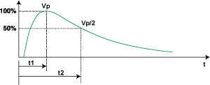
Figure 1. Lightning Transient Waveform
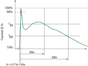
Figure 2. ESD Test Waveform
The exponential rise time of lightning is in the range 1.2μsec to 10μsec (essentially 10% to 90%) and the duration is in the range of 50μsec to 1000μsec (50% of peak values). ESD on the other hand, is a much shorter duration event. The rise time has been characterized at less than 1.0ns. The overall duration is approximately 100ns.
Why are Transients of Increasing Concern?
Component miniaturization has resulted in increased sensitivity to electrical stresses. Microprocessors for example, have structures and conductive paths which are unable to handle high currents from ESD transients. Such components operate at very low voltages, so voltage disturbances must be controlled to prevent device interruption and latent or catastrophic failures.
Sensitive microprocessors are prevelant today in a wide range of devices. Everything from home appliances, such as dishwashers, to industrial controls and even toys use microprocessors to improve functionality and efficiency.
Most vehicles now also employ multiple electronic systems to control the engine, climate, braking and, in some cases, steering, traction and safety systems.
Many of the sub- or supporting components (such as electric motors or accessories) within appliances and automobiles present transient threats to the entire system.
Careful circuit design should not only factor environmental scenarios but also the potential effects of these related components. Table 2 below shows the vulnerability of various component technologies.
| Device Type |
Vulnerability (volts) |
| VMOS |
30-1800 |
| MOSFET |
100-200 |
| GaAsFET |
100-300 |
| EPROM |
100 |
| JFET |
140-7000 |
| CMOS |
250-3000 |
| Schottky Diodes |
300-2500 |
| Bipolar Transistors |
380-7000 |
| SCR |
680-1000 |
Table 2: Range of device vulnerability.
ESD (Electrostatic Discharge)
Electrostatic discharge is characterized by very fast rise times and very high peak voltages and currents. This energy is the result of an imbalance of positive and negative charges between objects.
Below are some examples of the voltages which can be generated, depending on the relative humidity (RH):
- Walking across a carpet:
35kV @ RH = 20%; 1.5kV @ RH = 65%
- Walking across a vinyl floor:
12kV @ RH = 20%; 250V @ RH = 65%
- Worker at a bench:
6kV @ RH = 20%; 100V @ RH = 65%
- Vinyl envelopes:
7kV @ RH = 20%; 600V @ RH = 65%
- Poly bag picked up from desk:
20kV @ RH = 20%; 1.2kV @ RH = 65%
Referring to Table 2 on the previous page, it can be seen that ESD that is generated by everyday activities can far surpass the vulnerability threshold of standard semiconductor technologies. Figure 2 shows the ESD waveform as defined in the IEC 61000-4-2 test specification.
Inductive Load Switching
The switching of inductive loads generates high energy transients which increase in magnitude with increasingly heavy loads. When the inductive load is switched off, the collapsing magnetic field is converted into electrical energy which takes the form of a double exponential transient. Depending on the source, these transients can be as large as hundreds of volts and hundreds of Amps, with duration times of 400ms.
Typical sources of inductive transients are:
- Generator
- Motor
- Relay
- Transformer
These examples are extremely common in electrical and electronic systems. Because the sizes of the loads vary according to the application, the wave shape, duration, peak current and peak voltage are all variables which exist in real world transients. Once these variables can be approximated, a suitable suppressor technology can be selected.

Figure 3. Automotive Load Dump
Figure 3, shows a transient which is the result of stored energy within the alternator of an automobile charging system. A similar transient can also be caused by other DC motors in a vehicle. For example, DC motors power amenities such as power locks, seats and windows. These various applications of a DC motor can produce transients that are just as harmful to the sensitive electronic components as transients created in the external environment.
Lightning Induced Transients
Even though a direct strike is clearly destructive, transients induced by lightning are not the result of a direct strike. When a lightning strike occurs, the event creates a magnetic field which can induce transients of large magnitude in nearby electrical cables.
Figure 4, shows how a cloud-to-cloud strike will effect not only ove RHead cables, but also buried cables. Even a strike 1 mile distant (1.6km) can generate 70V in electrical cables.

Figure 4. Cloud-to-Cloud Lightning Strike
Figure 5, on the following page, shows the effect of a cloud-to-ground strike: the transient–generating effect is far greater.

Figure 5. Cloud-to-Ground Lightning Strike
Figure 6, shows a typical current waveform for induced lightning disturbances.

Figure 6. Peak Pulse Current Test Waveform
Technological Solutions for Transient Threats
Because of the various types of transients and applications, it is important to correctly match the suppression solution to the different applications. Littelfuse offers the broadest range of circuit protection technologies to ensure that you get the proper solution for your application. Please consult our online library of Application Notes and Design Notes for further information on common design issues encountered at https://www.littelfuse.com.